Posts Tagged ‘transistors’
Transistors – Voltage Regulation Part XVI
Monday, November 5th, 2012
Transistors – Voltage Regulation Part X
Monday, September 24th, 2012| Through the ages it’s been common practice to name important discoveries after those who discovered them. For example, James Watt was a mechanical engineer who improved the steam engine by finding a solution to the problem of steam condensing into water inside the engine, a phenomenon which resulted in the engine cooling and reducing its efficiency. Thus it was fitting that a metric unit of power, the watt, was named in his honor. Today we’ll become acquainted with the man behind the naming of the Zener diode, Clarence Zener, and take a look at his contributions with regard to the function of this electrical component.
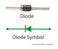
Last time we began our discussion on electrical components known as diodes and saw how they’re used on circuit paths to govern the flow of current. The Zener diode is a particular type of diode and a key component in transistorized voltage regulator circuits, as we’ll see later. For now, let’s see how it works. The symbol for the Zener diode is almost identical to that of a standard diode, introduced in my previous blog, but the Zener version has a bent line going through it resembling a distorted letter “z.” See Figure 1.
Figure 1
Electric current flows through the Zener Diode just as it does through a standard diode. But when the current flows in reverse, that’s where the similarity ends. See Figure 2. Figure 2
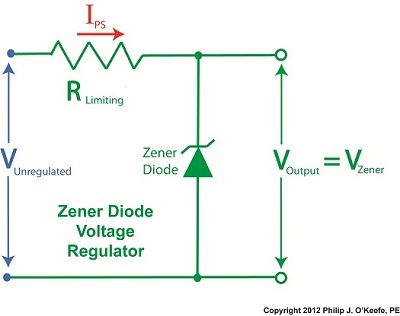
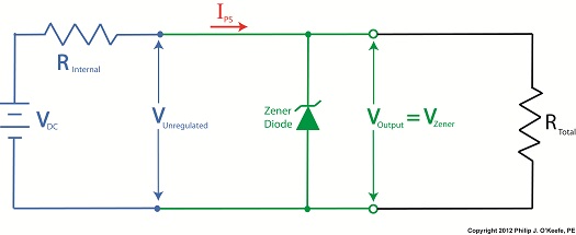
When current tries to flow in the reverse direction, the Zener diode acts as an electrical conductor and allows current to pass through it. In other words, it doesn’t block current flow as standard diodes do. At this point, you may be asking, “What’s so special about that?” Perhaps you’ve made the connection that it behaves no differently than a metal wire. But that isn’t entirely correct. You see, when current passes in the reverse direction through the Zener diode, it maintains a constant voltage. This is called the Zener Voltage and is denoted as VZener. The significance here is that within the circuit, any electronic component connected across the leads of a Zener diode will be supplied with a constant, unchanging voltage. Thus the Zener diode works as a voltage regulator, enabling devices connected to it to have smooth, uninterrupted operation at a constant voltage. It should be noted that this phenomenon only happens when the current flowing through the Zener diode is flowing in reverse. Next time we’ll look at a basic regulated power supply circuit to see how a Zener diode is incorporated in order to maintain a consistent output voltage. ____________________________________________ |


Transistors – Digital Control Interface, Part II
Sunday, June 24th, 2012| Not too long ago I was retained as an engineering expert to testify on behalf of a plaintiff who owned a sports bar. The place was filled with flat screen televisions that were plugged into 120 volt alternating current (VAC) wall outlets. To make a long story short, the electric utility wires that fed power to the bar were hit by a passing vehicle, causing the voltage in the outlets to increase well beyond what the electronics in the televisions could handle. The delicate electronics were not suited to be connected with the high voltage that suddenly surged through them as a result of the hit, and they overloaded and failed.
Similarly, lower voltage microprocessor and digital logic chips are also not suited to directly connect with higher voltage devices like motors, electrical relays, and light bulbs. An interface between the two is needed to keep the delicate electronic circuits in the chips from overloading and failing like the ill fated televisions in my client’s sports bar. Let’s look now at how a field effect transistor (FET) acts as the interface between low and high voltages when put into operation within an industrial product. I was once asked to design an industrial product, a machine which developed medical x-ray films, utilizing a microprocessor chip to automate its operation. The design requirements stated that the product be powered by a 120 VAC, such as that available through the nearest wall outlet. In terms of functionality, upon startup the microprocessor chip was to be programmed to first perform a 40-minute warmup of the machine, then activate a 12 volt direct current (VDC) buzzer for two seconds, signaling that it was ready for use. This sequence was to be initiated by a human operator depressing an activation button. The problem presented by this scenario was that the microprocessor chip manufacturer designed it to operate on a mere 5 VDC. In additional, it was equipped with a digital output lead that was limited in functionality to either “on” or “off” and capable of only supplying either extreme of 0 VDC or 5 VDC, not the 12 VDC required by the buzzer. Figure 1 illustrates my solution to this voltage problem, although the diagram shown presents a highly simplified version of the end solution.
Figure 1The illustration shows the initial power supplied at the upper left to be 120 VAC. This then is converted down to 5 VDC and 12 VDC respectively by a power supply circuit. The 5 VDC powers the microprocessor chip and the 12 VDC powers the buzzer. The conversion from high 120 VAC voltage to low 5 and 12 VDC voltage is accomplished through the use of a transformer, a diode bridge, and special transistors that regulate voltage. Since this article is about FETs, we’ll discuss transistor power supplies in more depth in a future article. To make things a little easier to follow, the diagram in Figure 1 shows the microprocessor chip with only one input lead and one output lead. In actuality a microprocessor chip can have dozens of input and output leads, as was the case in my solution. The input leads collect information from sensors, switches, and other electrical components for processing and decision making by the computer program contained within the chip. Output leads then send out commands in the form of digital signals that are either 0 VDC or 5 VDC. In other words, off or on. The net result is that these signals are turned off or on by the program’s decision making process. Figure 1 shows the input lead is connected to a pushbutton activated by a human. The output lead is connected to the gate (G) of the FET. The FET is shown in symbolic form in green. The FET drain (D) lead is connected to the buzzer and its source (S) lead terminates in connection to electrical ground to complete the electrical circuit. Remember, electric current naturally likes to flow from the supply source to electrical ground within circuits, and our scenario is no exception. Next time we’ll see what happens when someone presses the button to put everything into action.
____________________________________________ |


